- 您现在的位置:买卖IC网 > Sheet目录477 > MICRF501BLQ TR (Micrel Inc)TXRX SGL 300-600MHZ 44-LQFP
�� �
�
�MICRF501�
�signals.� The� receive� mode� loop� filter� comprises� C115,� C116,�
�R109,� R101� and� C101.�
�Modulation� Outside� PLL� (Open� Loop)�
�In� this� mode� the� charge� pump� output� is� tri-stated.� The� loop� is�
�open� and� will� therefore� not� track� the� modulation.� This� means�
�that� the� loop� filter� can� have� a� relatively� high� bandwidth,� which�
�give� short� switching� times.� However,� the� loop� voltage� will�
�decrease� with� time� due� to� current� leakage.� The� transmit� time�
�will� therefore� be� limited� and� is� dependent� on� the� bandwidth� of�
�the� loop� filter.� High� bandwidth� gives� low� capacitor� values� and�
�the� loop� voltage� will� decrease� faster,� which� gives� a� shorter�
�transmit� time.�
�The� loop� is� closed� until� the� PLL� is� locked� on� the� desired�
�frequency� and� the� power� amplifier� is� turned� on.� The� loop�
�immediately� opens� when� the� modulation� starts.� The� loop� will�
�not� track� the� modulation,� but� the� modulation� still� needs� to� be�
�DC� free� due� to� the� AC� coupling� in� the� modulation� network.�
�Transmit�
�Power� Amplifier� (PA)�
�The� power� amplifier� is� biased� in� class� AB.� The� last� stage� has�
�an� open� collector,� and� an� external� load� inductor� (L5)� is�
�therefore� necessary.� The� DC� current� in� the� amplifier� is�
�adjusted� with� an� external� bias� resistor� (R14).� A� good� starting�
�point� when� designing� the� PA� is� a� 1.5k� ?� bias� resistor� which�
�gives� a� bias� current� of� approximately� 50� μ� A.� This� will� give� a�
�bias� current� in� the� last� stage� of� about� 15mA.� R14� is� optimized�
�to� 1k� ?� ,� as� shown� in� the� application� circuit.�
�The� impedance� matching� circuit� will� depend� on� the� type� of�
�antenna� used,� but� should� be� designed� for� maximum� output�
�power.� For� maximum� output� power� the� load� seen� by� the� PA�
�must� be� resistive� and� should� be� about� 100� ?� .� The� output�
�power� is� programmable� in� eight� steps,� with� approximately�
�3dB� between� each� step.� This� is� controlled� by� bits� Pa2� -� Pa0.�
�To� prevent� spurious� components� from� being� transmitted� the�
�PA� should� be� switched� on/off� slowly,� by� allowing� the� bias�
�current� to� ramp� up/down� at� a� rate� determined� by� the� external�
�capacitor� C25� connected� to� Pin� 24.� The� ramp� up/down�
�current� is� typically� 1.1� μ� A,� which� makes� the� on/off� rate� for� a�
�2.8V� power� supply� 2.6� μ� s/pF.� Turning� the� PA� on/off� affects� the�
�PLL.� Therefore� the� on/off� rate� must� be� adjusted� to� the� PLL�
�bandwidth.�
�PA� Buffer�
�A� buffer� amplifier� is� connected� between� the� VCO� and� the� PA�
�Micrel�
�stabilizes� the� overall� dc� feedback� loop,� which� has� a� large� low�
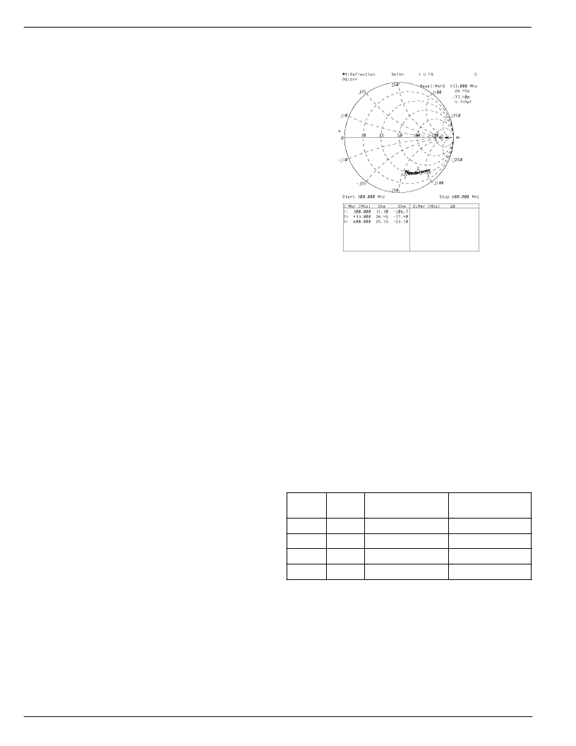
�frequency� loop� gain.� Figure� 8� shows� the� input� impedance� of�
�the� LNA.�
�Figure� 8.� Input� Impedance�
�Input� matching� is� very� important� to� get� high� receive� sensitiv-�
�ity.� The� LNA� can� be� bypassed� by� setting� bit� LNA� to� ‘� 1� ’� .� This�
�is� useful� for� very� strong� signal� levels.� The� RSSI� signal� can� be�
�used� to� drive� a� microcontroller� to� create� a� subroutine� when� a�
�strong� income� signal� is� present� to� bypass� the� LNA.� This� will�
�increase� the� dynamic� range� by� approximately� 25dB.�
�The� mixers� have� a� gain� of� about� 15dB� at� 434MHz.� The�
�differential� outputs� of� the� mixers� are� available� at� Pins� 34,� 35�
�and� at� Pins� 38,� 39.� The� output� impedance� of� each� mixer� is�
�about� 30k� ?� .�
�Sallen-Key� Filter� and� Preamplifier�
�Each� channel� includes� a� preamplifier� and� a� prefilter,� which� is�
�a� three-pole� elliptic� Sallen-Key� lowpass� filter� with� 20dB�
�stopband� attenuation.� It� protects� the� following� gyrator� filter�
�from� strong� adjacent� channel� signals.� The� preamplifier� has� a�
�gain� of� 35dB� and� output� voltage� swing� is� about� 200mV� PP� .�
�The� third� order� Sallen-Key� lowpass� filter� is� programmable� to�
�four� different� cut-off� frequencies� according� to� the� table� below:�
�Fc1� Fc0� Cut-Off� Frequency� Recommended�
�(kHz)� Channel� Spacing�
�0� 0� 10� ±� 2.5� 25kHz�
�0� 1� 30� ±� 7.5� 100kHz�
�to� ensure� that� the� input� signal� of� the� PA� has� sufficient�
�1�
�0�
�60� ±� 15�
�200kHz�
�amplitude� to� achieve� the� desired� output� power.� This� buffer�
�can� be� bypassed� by� setting� the� bit� Gc� to� 0.�
�Receive�
�Front� End� (LNA� and� Mixers)�
�A� low� noise� amplifier� in� the� RF� receiver� is� used� to� boost� the�
�incoming� signal� prior� to� the� frequency� conversion� process.�
�This� is� important� in� order� to� prevent� mixer� noise� from� domi-�
�nating� the� overall� front� end� noise� performance.� The� LNA� is� a�
�two� stage� amplifier� and� has� a� nominal� gain� of� 25dB� at�
�434MHz.� The� LNA� has� a� dc� feedback� loop,� which� provides�
�bias� for� the� LNA.� The� external� capacitor� C26� decouples� and�
�1� 1� 200� ±� 50� 700kHz�
�For� the� 10kHz� cut-off� frequency� the� first� pole� must� be� gener-�
�ated� externally� by� connecting� a� 330pF� capacitor� between� the�
�outputs� of� each� mixer.�
�As� the� cut-off� frequency� of� the� gyrator� filter� can� be� set� by�
�varying� an� external� resistor,� the� optimum� channel� spacing�
�will� depend� on� the� cut-off� frequencies� of� the� Sallen-Key� filter.�
�The� table� above� shows� the� recommended� channel� spacing�
�depending� on� the� different� bit� settings.�
�MICRF501�
�12�
�March� 2003�
�发布紧急采购,3分钟左右您将得到回复。
相关PDF资料
MICRF505DEV1
KIT DEV RADIOWIRE 850-950MHZ
MICRF506DEV1
EVAL BOARD EXPERIMENTAL MICRF506
MICRF507YML TR
TXRX FSK LOW PWR W/AMP 32MLF
MICRF600DEV1
KIT DEV RADIOWIRE 902-928MHZ
MK01-C
SENSOR REED SPST-NO SMD
MK01-H
SENSOR REED SPDT-CHANGE SMD
MK02/0-1A66-500W
SENSOR REED SPST-NO
MK02/6-0
SENSOR REED PCB 24MM T/H
相关代理商/技术参数
MICRF501EVAL1
功能描述:EVAL BOARD EXPERIMENTAL MICRF501 RoHS:否 类别:RF/IF 和 RFID >> RF 评估和开发套件,板 系列:RadioWire® 标准包装:1 系列:- 类型:GPS 接收器 频率:1575MHz 适用于相关产品:- 已供物品:模块 其它名称:SER3796
MICRF505
制造商:MICREL 制造商全称:Micrel Semiconductor 功能描述:868MHz and 915MHz ISM Band Transceiver
MICRF505_07
制造商:MICREL 制造商全称:Micrel Semiconductor 功能描述:850MHz and 950MHz ISM Band Transceiver
MICRF505BML
制造商:Rochester Electronics LLC 功能描述: 制造商:RF Micro Devices Inc 功能描述:
MICRF505BML TR
功能描述:TXRX ISM 868-915MHZ 32-MLF RoHS:否 类别:RF/IF 和 RFID >> RF 收发器 系列:- 产品培训模块:Lead (SnPb) Finish for COTS
Obsolescence Mitigation Program 标准包装:30 系列:- 频率:4.9GHz ~ 5.9GHz 数据传输率 - 最大:54Mbps 调制或协议:* 应用:* 功率 - 输出:-3dBm 灵敏度:- 电源电压:2.7 V ~ 3.6 V 电流 - 接收:* 电流 - 传输:* 数据接口:PCB,表面贴装 存储容量:- 天线连接器:PCB,表面贴装 工作温度:-25°C ~ 85°C 封装/外壳:68-TQFN 裸露焊盘 包装:管件
MICRF505DEV1
功能描述:射频开发工具 MICRF505 Evaluation Kit - For experimental use only
RoHS:否 制造商:Taiyo Yuden 产品:Wireless Modules 类型:Wireless Audio 工具用于评估:WYSAAVDX7 频率: 工作电源电压:3.4 V to 5.5 V
MICRF505DEV1
制造商:Micrel Inc 功能描述:KIT MICRF505 EVALUATION
MICRF505L
制造商:MICREL 制造商全称:Micrel Semiconductor 功能描述:850MHz and 950MHz ISM Band Transceiver